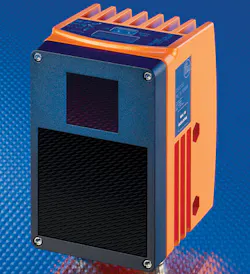
Now, ifm efector Inc., an Exton, Pa.-based manufacturer of sensors and controls, is claiming a “breakthrough” for the industrial automation space with a new 3D Image Sensor based on time-of-flight technology applied through an array of light-sensitive pixels and associated electronics housed on a single silicon chip. The integrated approach sets a new benchmark for price/performance in reliable 3D object detection, ifm claims.
Garrett Place, ifm effector product manager, likens the new sensor to an electronic version of an old-fashioned “pin art” toy, in which an object is pushed into an array of pins, leaving a 3D image of the object formed by the pins. “That’s exactly what this does,” says Place. “It creates a 3D image.”
In this case, however, the image is created electronically, based on time-of-flight distance measurements applied to each of 3,072 “Smart Pixels” on the sensor’s 0.25 millimeter (mm)-square silicon integrated circuit. The pixels are arranged in a 64-by-48 array on the chip, which uses so-called Photonic Mixing Device (PMD) technology to calculate distances for each of the pixels.
When the sensor is in operation, modulated infrared (IR) light is emitted from light emitting diodes (LEDs) contained in the sensor’s 42-by-62-by-42 mm metal housing. The reflected light is then focused through lenses and received by the PMD chip, which is also connected to the modulation source. The electrons are converted into photons and are separated inside the optically sensitive area of the PMD array chip in relation to an electrical reference signal. This built-in functionality means that the sensor can pre-process the signal, eliminating the need for expensive high-speed electronics, ifm says.
Relating the phase difference measured by each pixel to the speed of light provides the distance traveled by light falling onto the detector. The phase shift of the light is then compared to the reference signal and sent from the chip as the representative distance for each of the pixels. Information from all of the pixels is then combined to create a 3D image.
Key features of the 3D Image Sensor include patented technology that can suppress the effects of ambient lighting, which is particularly important for the variable lighting conditions found in industrial environments, says Place. Built-in color-correction capability also eliminates potential problems related to differing reflectivity of IR light throughout the color spectrum, he adds.
But the biggest “breakthrough” achieved with the technology is its price/performance, which sets a new benchmark for reliable 3D object detection in the industrial space, Place says. List price for the 3D Image Sensor is $1,450. Other industrial 3D systems such as light detection and ranging (LIDAR), stereo-vision and long-range radars are typically 300 percent to 400 percent more expensive, according to ifm. “This could really revolutionize many different applications inside the industrial marketplace. To be able to take 3,072 points of data at one time for under $1,500 list is unheard of,” Place contends.
Applications
The 3D Image Sensor’s field of view can range up to about three-by-two meters, says Place. Maximum sensing range is six meters. He foresees a variety of industrial applications for the technology. These include palletizing and depalletizing, in which a high-mounted sensor can detect whether a pallet layer is complete or incomplete, for example, or if a box has been left on the top layer of a pallet. Other applications may involve bulk material level sensing, where the 3D sensor can see the “hills and valleys” caused by shifting materials within a large hopper or bin.
The 3D Image Sensor will be available in two versions, says Place. The “sensor” version includes canned algorithms for various volume, distance and level detection applications, and comes with a Set-up Wizard. A second “camera” version is freely programmable by the user for specialized tasks, Place notes. The 3D Image Sensor was scheduled for introduction during the first week of May.
Subscribe to Automation World's RSS Feeds for Columns & Departments
About the Author
Wes Iversen
Managing Editor

Leaders relevant to this article:
